Silicon carbide (SIC), one of the preferred materials in semiconductor manufacturing, has become a key part of the load-bearing and positioning components in semiconductor manufacturing equipment due to its high hardness, low thermal expansion, ultra-high rigidity and excellent chemical inertness, such as (carrier tray plate, wafer chuck, needle chuck, ring chuck, slot chuck, ceramic needle chuck, wafer chuck table, etc.) to help the efficient and high-yield operation of detection, bonding, metrology and lithography processes
SiC Parts Advantages
- Low thermal expansion coefficient: 4.0×10⁻⁶/K, well matched with silicon wafer (2.6×10⁻⁶/K)
- Ultra-high rigidity and wear resistance: close to the hardness of single crystal grinding wheel.
- Stable support of mechanical load after processing, long service life.
- Chemical inertness and clean compatibility: resistant to photoresist solvents and common chemical reagents
- Nanoscale super plane: surface flatness can reach ≤0.01–0.05μm, roughness Ra≤0.3–1nm
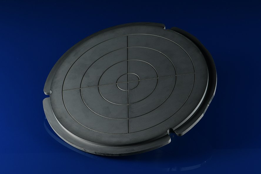
SiC Core Parts
| 组件 | Primary Function | Wafer Size | Flatness (Global) | Surface Roughness (Ra) | Machining Tolerance | Vacuum Hole / Clamping Method |
| SiC Carrier Tray Plate | Wafer storage and short-distance transfer | 6″ / 8″ / 12″ | ≤ 0.05 μm | ≤ 1 nm | ± 5 μm | Optional vacuum suction hole array |
| SiC Wafer Chuck | Platform for lithography, inspection, bonding | 12″ | ≤ 0.02 μm | ≤ 0.5 nm | ± 2 μm | Evenly distributed vacuum holes |
| SiC Pin Chuck | Point support for die or small wafers | Custom size | ≤ 0.05 μm | ≤ 1 nm | Pin height ± 1 μm | Dual-mode: mechanical / vacuum |
| SiC Ring Chuck | Support for ring-shaped or custom wafers | Custom diameter | ≤ 0.03 μm | ≤ 0.8 nm | ± 3 μm | Vacuum-sealed ring groove |
| SiC Groove Chuck | V/U groove support for curved or odd-shaped wafers | Custom width | ≤ 0.04 μm | ≤ 0.8 nm | Groove width ± 2 μm | Vacuum channel at groove base |
| SiC Ceramic Needle Gripper | Precision gripping of probes or micro parts | - | Needle tip ≤ 0.02 μm | ≤ 0.5 nm | Pin pitch ± 2 μm | Mechanical grip / optional vacuum |
| SiC Wafer Chuck Stage | High-precision XYZ motion and nano positioning | 12″ | ≤ 0.01 μm (ultra-flat) | ≤ 0.3 nm | Parallelism ≤ 50 nm | Hybrid vacuum & mechanical clamping |
Note: All parts can be customized according to customer requirements
SiC Parts Application
- Wafer inspection equipment probe card fixture, carrier, carrier and transfer arm, etc.
- Bonding equipment hot press plate, thermocouple seat, etc.
- Measuring equipment turntable bearing seat, chuck, bracket, etc.
- Photolithography machine alignment table, aperture bracket, etc.
Semiconductor Ceramics Manufacturers
As a specialized semiconductor ceramics manufacturer, we provide ultra-flat, high-purity silicon carbide (SiC) parts engineered for demanding processes — from wafer inspection, bonding, metrology to photolithography.