Single Crystal Silicon
It is a silicon material with orderly atomic arrangement and high purity.
Single Crystal Silicon is a silicon material with a complete crystal structure. It can be doped into N-type silicon or P-type silicon to meet different application requirements and become a core material in the semiconductor and optical fields.
Advantages
The crystal structure is complete and defect-free
High electron mobility
High temperature resistance, suitable for harsh environments
Bending resistance and wear resistance
Controllable purity, divided into N type and P type to meet different application requirements
Can be ultra-precision processed
Applications
- Semiconductor chips
- Pressure sensors
- Transistors and diodes
- Photovoltaic cells
- Optical components
- Microelectromechanical systems (MEMS)
- Gyroscopes
- Wafer packaging
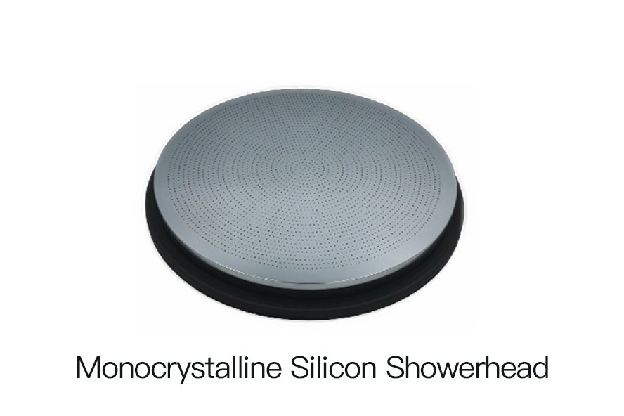
- Monocrystalline Silicon Spray Plate
Single Crystal Silicon Properties
| Crystal Structure | Lattice type | — | Diamond cubic (Fd3̅m) |
| Lattice constant | a (Å) | 5.431 | |
| Physical Properties | Density | ρ (g/cm³) | 2.329 |
| Melting point | Tₘ (°C) | 1414 | |
| Coefficient of thermal expansion | α (10⁻⁶ K⁻¹) | 2.6 @ 25–300 °C | |
| Mechanical Properties | Young’s modulus | E (GPa) | 130–188 |
| Poisson’s ratio | ν | 0.22 | |
| Fracture toughness | K_IC (MPa·m½) | 0.6–0.9 | |
| Thermal Properties | Thermal conductivity | κ (W/m·K) | 148 @ 300 K |
| Specific heat capacity | C_p (J/kg·K) | 700 @ 300 K | |
| Electrical Properties | Bandgap energy | E_g (eV) | 1.12 @ 300 K |
| Intrinsic carrier concentration | n_i (cm⁻³) | 1 × 10¹⁰ @ 300 K | |
| Relative permittivity | ε_r | 11.7 | |
| Intrinsic resistivity | ρ_i (Ω·cm) | ~2 × 10⁵ | |
| Doped resistivity | ρ_d (Ω·cm) | 0.001–10 (depending on doping) | |
| Carrier Mobility | Electron mobility | μ_n (cm²/V·s) | ≈1,350 @ 300 K |
| Hole mobility | μ_p (cm²/V·s) | ≈450 @ 300 K | |
| Optical Properties | Refractive index | n (@ 632.8 nm) | 3.88 |
| Absorption edge | λ_g (μm) | 1.1 | |
| Surface & Interface | Surface energy | γ (J/m²) | 1.24 |
| Interface state density | D_it (cm⁻²·eV⁻¹) | 10¹⁰–10¹¹ |
Note: All values are typical at room temperature (≈300 K). Actual values may vary slightly with crystal orientation, doping level, and measurement method.
Single Crystal Silicon Machining
Single Crystal Silicon is a common material in semiconductors with excellent properties. Jundro Ceramics is an ultra-hard materials manufacturer that can provide precision processing of N-type silicon and P-type silicon. With our rich experience and diverse equipment, we can perfectly meet your application needs.
Need to customize Single Crystal Silicon? Contact us today to speak with our materials experts to create a solution that exceeds expectations!
FAQ
Single crystal silicon is a highly pure material with a uniform crystal structure, widely used in semiconductors, optics, and MEMS applications.
We can machine wafers, blocks, rings, plates, lenses, windows, and custom precision parts according to drawings.
Typical tolerances are ±0.01 mm, and high-precision parts can reach ±0.001 mm with optical-grade surfaces.
Common applications include semiconductor devices, MEMS components, optical windows, infrared parts, precision fixtures, and high-stability structural components.