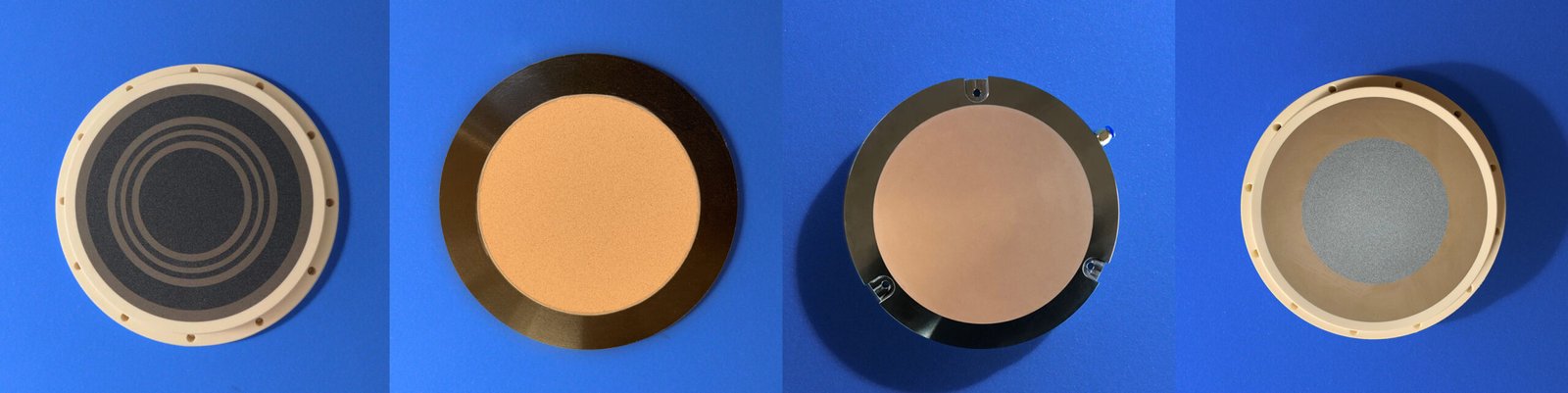
Porous ceramic chucks are a type of vacuum chuck that uses micron/submicron interconnected channels to achieve uniform negative pressure adsorption. Compared to traditional grooved or perforated metal chucks, porous ceramics can provide uniform adsorption across the entire surface without localized depressions, greatly reducing the deformation and localized stress caused by thin wafers/wafers being “sucked into the grooves.” This is particularly important for precision processes such as ultra-thin wafers.
メリット
Uniform Adsorption: Micropores are distributed throughout to avoid localized warping caused by adsorption.
Low Particle/Cleanroom Compatible: High-purity materials are used to meet the particle and impurity requirements of cleanroom processes.
Chemical and Thermal Stability: Depending on the material selection (alumina/SiC), it is compatible with high-temperature, plasma, or chemical cleaning processes.
Customizable Pore Size and Porosity: Pore size (typically 1–120 μm) and open porosity (e.g., 30–50%) can be controlled using porogens or sacrificial phases to balance adsorption strength and particulate filtration performance.
Commonly used materials
High-purity aluminum oxide (Al₂O₃): It can achieve excellent surface flatness, is cost-friendly and process-friendly, and is suitable for most semiconductor scenarios.
Silicon carbide (SiC/SiSiC): Higher thermal stability and mechanical strength, suitable for high temperature or heavy load grinding and CVD environments
Ceramic composite or special formulation: Special formulation or surface treatment (coating, sealing) can be used to meet the needs of particle control, thermal conductivity or electrical conductivity
Specifications
| Item | Example Value / Description |
| 素材 | 99.5% Al₂O₃ / SiC (optional) |
| Pore Size | 1 μm / 5 μm / 15 μm / 25 μm (customizable). Commonly ≤25 μm for optical/thin wafer use (photomachining.com) |
| 多孔性 | 30–50% (adjustable depending on application) (xminnovacera.en.made-in-china.com) |
| Flatness (TTV) | 1–10 μm (depending on size and machining grade) |
| Maximum Operating Temp | Al₂O₃ ~1000 °C (depending on sintering and composition), SiC higher (xminnovacera.en.made-in-china.com) |
| Common Size/Shape | Circular 4″–12″, square, or customized shapes |
申し込み
- Suction cups for wafer grinding/backgrinding and dicing machines.
- Scratch-free fixturing in optical/lens processing and polishing.
- Probe stations/inspection platforms (uniform adsorption, tiny sample fixation).
よくあるご質問
Will porous ceramic suction cups cause particles to be sucked into the holes?
Good process and post-processing (high purity materials, controlled sintering, cleaning and vacuum packaging) can reduce the risk of particles to a very low level; if necessary, smaller pore size or surface sealing/coating can be selected to further reduce the risk.
How to choose the aperture?
For ultra-thin/optical workpieces, select ≤25 μm; for fast vacuuming or large-area handling, choose a larger aperture to reduce airflow resistance
Can porous ceramic chucks replace electrostatic chucks?
The two complement each other; porous ceramics are suitable for non-contact uniform vacuum adsorption (no electrostatic damage), while electrostatic chucks have advantages in certain automatic loading and temperature control scenarios. You can choose based on yield, material and equipment integration.
 English
  简体中文
简体中文  Español
  Deutsch (Sie)
  日本語
日本語