In semiconductor applications, many components that can withstand high temperatures, high vacuum, and strong chemical corrosion are required to ensure stable operation of the equipment. For example, the aluminum oxide ceramic arm is responsible for accurately aligning the wafer position for the next processing steps (such as thin film deposition, photolithography, etc.). Advanced ceramics are widely used in semiconductors. The following are its key material types and typical applications.
Key Advanced Ceramic Materials
Aluminum Nitride Ceramic
- High thermal conductivity and electrical insulation properties, perfect thermal match to silicon
- Semiconductor packaging substrates, IGBT modules, and RF device carriers for efficient heat dissipation.
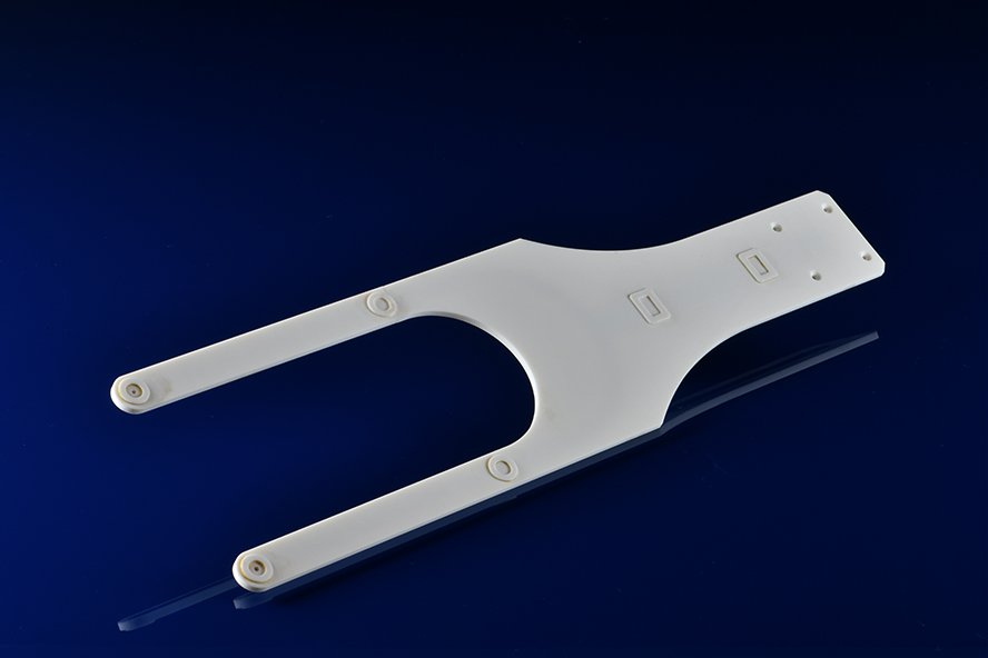
Alumina Ceramic
- High mechanical strength, corrosion resistance, and moderate cost.
- Vacuum chamber liner, plasma etching machine nozzle, wafer transfer robot arm parts in semiconductor equipment
Silicon Carbide Ceramic
- Ultra-high temperature stability (>1600℃), wear resistance and corrosion resistance
- Epitaxial growth reactor components, thermal field materials for high temperature CVD (chemical vapor deposition) equipment
- High fracture toughness, excellent thermal shock resistance
- Precision bearings for photolithography machines and wafer cutting blades to reduce vibration and wear during processing
Semi-Conducting Ceramics Examples


Machining Technology Challenges
Precision machining: The brittleness of ceramics requires ultra-precision machining technology (such as laser cutting and diamond grinding) to achieve micron-level tolerances and complex structures.
Material composites: Develop ceramic-metal composite substrates (such as AlSiC) to balance heat dissipation and mechanical strength requirements.
Emerging demands: With the rise of third-generation semiconductors (GaN, SiC), high-voltage and high-frequency ceramic packaging solutions have become a research and development focus.
Contact us via form
All tolerances can be improved based on the size, shape, and geometry of the precision ceramic components to perfectly match your equipment and specific requirements.