The semiconductor industry has always been the most widely used application of ceramics. Especially with the continuous upgrading of semiconductor equipment and technology, equipment manufacturers need high-performance and highly reliable materials for demanding processes such as deposition, etching, and photolithography. Alumina ceramics, due to their excellent thermal stability, insulation, and cost, help semiconductor equipment operate stably.
Core Applications of Alumina in Semiconductor Manufacturing
High-purity alumina is integrated into nearly every stage of wafer fabrication. Key roles include:
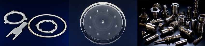
Alumina substrates for semiconductor devices
Alumina insulators for semiconductor applications
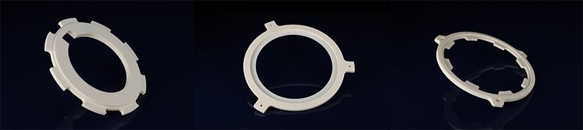
Precision machined alumina parts for semiconductor tools
Alumina ceramic fixtures for semiconductor fabrication
Alumina isolation rings for semiconductor machinery
These components withstand demanding environments—high temperature, plasma exposure, and corrosive chemicals—making alumina an indispensable material for front-end and back-end semiconductor processing.
Material Property Advantages: Why Alumina Outperforms Metal and Quartz
The semiconductor industry increasingly adopts alumina to replace traditional metals and quartz due to the following material advantages:
High temperature resistance for thermal processing chambers
High dielectric strength for RF insulation components
Wear resistance and hardness, extending equipment lifespan
Corrosion resistance, essential for CVD, PVD, and etching systems
Vacuum compatibility, reducing outgassing and contamination
These benefits make high-purity alumina ceramics for semiconductor manufacturing the preferred choice for equipment OEMs seeking stability and long-term reliability.
Manufacturing & Machining: High-Precision Alumina Components for Semiconductor Tools
Modern semiconductor tools require ceramics with tight tolerances, complex geometries, and flawless surface integrity. Advanced CNC capabilities enable:
Custom machined alumina parts for semiconductor industry
CNC machining alumina ceramics for semiconductor applications
Tight-tolerance alumina machining for semiconductor components
5-axis machining of alumina ceramics for semiconductor systems
With tolerances down to microns and exceptional surface finishes, precision machining ensures each component performs consistently within high-vacuum, high-temperature, and plasma-rich environments.
Industry-Specific Applications: Where Alumina Delivers Performance
Alumina plays critical roles in advanced semiconductor equipment such as:
Semiconductor etching equipment – alumina ceramic spacers, nozzles, chamber liners
PVD & CVD equipment – corrosion-resistant alumina insulators and shields
Ion implantation machines – high-strength alumina insulators
Lithography systems – alumina alignment fixtures and stabilization components
Wafer handling tools – alumina guides, pins, and precision structural components
In each application, alumina’s thermal resistance, electrical insulation, and dimensional stability directly contribute to better process consistency and yield.
Conclusion
Alumina ceramics have become foundational materials in the semiconductor industry due to their unmatched combination of thermal stability, dielectric strength, mechanical durability, and vacuum compatibility. From custom machined alumina parts to alumina substrates and RF insulation components, alumina ensures precision, safety, and reliability throughout wafer fabrication.