In the semiconductor industry, most people are unaware of the materials that enable the ultra-high precision and performance of today’s electronic devices. These materials play specific roles in key processes such as wafer fabrication, photolithography, etching, and packaging.
Silicon (Si): The Foundation of Modern Semiconductors
Silicon remains the foundation of semiconductor technology. Its ability to act as both an insulator and a conductor under precise doping makes it ideal for forming integrated circuits. High-purity monocrystalline silicon wafers are used as the starting point for almost all chips, supporting microfabrication at the nanometer scale.
Key advantages:
Excellent electrical and thermal characteristics
Abundant and cost-effective
Well-established processing technology

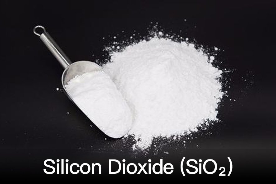
Silicon Dioxide (SiO₂): Insulation and Protection
Silicon dioxide, commonly known as silica, is used as a dielectric layer and surface passivation material. It provides insulation between conductive layers, protects the wafer from contamination, and ensures long-term device reliability. Thin films of SiO₂ are typically grown through thermal oxidation or chemical vapor deposition (CVD).
Applications:
Gate oxide in MOSFETs
Interlayer dielectric in integrated circuits
Protective coatings
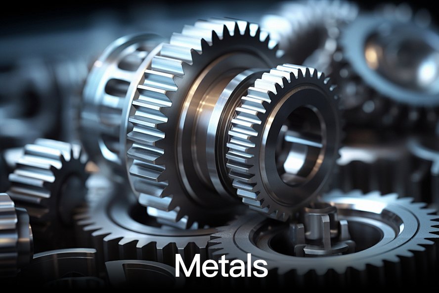
Metals: Conductive Paths for Electrical Signals
Metals such as aluminum, copper, tungsten, and titanium are widely used in semiconductor interconnects, electrodes, and contact layers. They provide the conductive pathways necessary for signal transmission and power delivery within microchips. Copper, in particular, has become the dominant choice due to its low resistivity and excellent electromigration resistance.
Common metals and their uses:
Copper (Cu): Interconnects and wiring
Tungsten (W): Via and contact filling
Aluminum (Al): Older interconnect technology and bonding pads
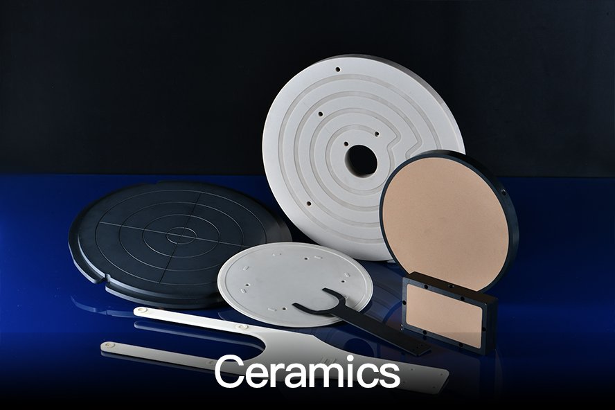
Ceramics: High-Performance Materials for Extreme Environments
Ceramic materials are indispensable in semiconductor manufacturing due to their exceptional thermal, electrical, and mechanical properties. They are used in critical components that demand high precision, stability, and resistance to harsh process conditions.
Common ceramic materials:
Aluminum oxide (Al₂O₃): Excellent electrical insulation and chemical resistance
Aluminum nitride (AlN): High thermal conductivity and electrical insulation
Silicon carbide (SiC): Outstanding strength and plasma resistance
Macor and Zerodur: Machinable ceramics used for precision fixtures and alignment components
Applications in semiconductor manufacturing:
Wafer carriers, electrostatic chucks, and heater stages
Plasma-resistant parts in etching and deposition equipment
High-precision insulating components in lithography and inspection systems
The reliability and dimensional stability of advanced ceramics make them essential for maintaining tight process control and ensuring product quality in high-vacuum or high-temperature environments.
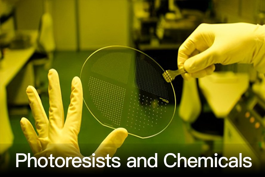
Photoresists and Chemicals: Patterning with Precision
Photoresists and process chemicals are key to defining the intricate patterns on semiconductor wafers. Photoresists react to ultraviolet or extreme ultraviolet (EUV) light, enabling precise pattern transfer during photolithography. Accompanying chemicals such as etchants, developers, and cleaning agents play critical roles in shaping and refining microstructures.
Types of photoresists:
Positive resists: Exposed regions become soluble and are removed
Negative resists: Exposed regions harden and remain after development
Conclusion
Semiconductor manufacturing is a complex interplay of materials science and precision engineering. From silicon wafers and conductive metals to advanced ceramics and chemical compounds, each material contributes uniquely to performance, reliability, and miniaturization.
As device geometries continue to shrink and process conditions grow more demanding, technical ceramics will play an increasingly vital role — ensuring stability, insulation, and thermal management in next-generation semiconductor equipment and components.