Fused Silica Glass
Very low coefficient of thermal expansion (approximately 0.5 × 10⁻⁶ /°C)
| Material | Fused Silica Glass |
| Density | 2.20 g/cm³ |
| Roughness | Ra0.002μm |
| Maximum size | ф500*50mm |
Introduction
Fused Silica Glass is widely used in high-tech fields such as semiconductors, optics, and scientific research due to its excellent physical and chemical properties. It is composed of amorphous materials of high-purity silicon dioxide SiO₂ (>99.9%), which does not contain other oxides and avoids impurities. At the same time, Fused Silica has strong resistance to acids, alkalis and most corrosive substances, and is suitable for extreme chemical environments. The following is a detailed introduction to its characteristics and applications.
Fused Silica Glass Advantages
✅ High purity >99.9% SiO₂
✅ Extremely low thermal expansion coefficient (0.5 × 10⁻⁶ /°C) and strong thermal shock resistance
✅ High resistivity
✅ Strong resistance to chemicals
✅ High transmittance from deep ultraviolet to infrared (175 nm ~ 2500 nm), suitable for optical applications
✅ High mechanical strength, precision polishable surface
Application
✅ Photolithography masks, photolithography machine lenses, wafer carriers, heat treatment boats, cavity windows
✅ Ultraviolet lenses, laser windows, reflector substrates
✅ Infrared/ultraviolet windows, high-speed aircraft windows
✅ Quartz cuvettes, laser cavity lenses
✅ Optical path components for spectrometers and chromatographs
✅ High-temperature gas sensor windows
✅ Microstructure devices, optical trap structures, vacuum cavity windows
✅ Interferometers, gyroscope substrates
Fused Silica Glass Properties
Material Properties
| Property | Unit | Fused Silica Glass |
| Density | g/cm³ | 2.2 |
| Bending Strength | MPa | 80 |
| Compressive Strength | MPa | 1100 |
| Elastic Modulus | GPa | 220 |
| Poisson’s Ratio | – | 0.17 |
| Young’s Modulus | GPa | 72 |
Thermal Properties
| Property | Unit | Fused Silica Glass |
| Thermal Conductivity | W/m·K | 1.38 |
| Melting Point | °C | 1730 |
| Maximum Operating Temperature | °C | 1200 |
| Linear Expansion Coefficient | 10⁻⁶/K | 0.55 |
Electrical Properties
| Property | Unit | Fused Silica Glass |
| Dielectric Constant | 1 MHz | 3.75 |
| Breakdown Voltage | V/cm | 400 |
| Dielectric Loss | 1 MHz | < 0.0004 |
| Resistivity | Ω·cm | > 10¹⁸ |
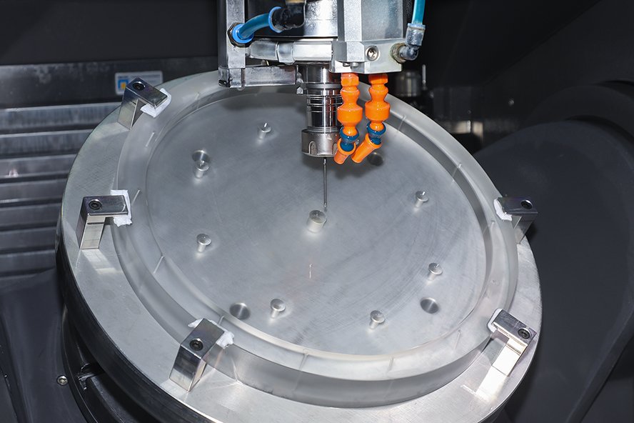
Fused Silica Glass Machining
Fused Silica Glass Manufacturer
High-Purity Fused Silica Glass Manufacturer & Precision Machining Expert
We are a professional manufacturer of high-purity fused silica glass, offering integrated services from material supply to precision CNC machining. With advanced 3-axis, 4-axis, and 5-axis machining capabilities, we produce custom components with ultra-tight tolerances (±0.001 mm), optical-grade polishing (up to 1/20λ), and complex geometries.
Our fused silica parts are widely used in semiconductors, optics, aerospace, analytical instruments, and scientific research. Backed by ISO 9001 and ISO 14001 certifications, we ensure stable quality, fast delivery, and technical support tailored to your critical applications.
FAQ
No.
Fused silica refers to amorphous SiO₂. Quartz is crystalline.
They behave differently under heat and stress.
What Is JGS1 Fused Silica?
JGS1 Fused Silica is a UV-grade optical quartz material characterized by high purity, excellent UV transmittance (185–2500 nm), and superior thermal stability. It is one of the three grades defined by China’s GB/T 31447.1 standard for optical fused silica (JGS1, JGS2, JGS3).
JGS1: UV-grade, best for deep-UV and precision optics.
JGS2: Standard optical grade for visible–IR.
JGS3: IR-grade, ideal for thermal or infrared applications.
Lithography & Direct Writing, Exposure windows, mask holders
Photoresist Coating & Developing、Quartz coating covers
Wet Process Equipment, Wafer carriers and boats
Dry Etching Equipment, Quartz chamber liners, Electrode covers
Thin Film Deposition (CVD, PECVD, ALD), Chamber liners
For more semiconductor applications, please check this article (In 3 Minutes: The Complete Applications of Fused QuartzGlass in Semiconductor Equipment)
- High-Precision Capabilities:
- Complex shapes: tolerances up to ±0.01 mm
- Cylindrical/shaft components: tolerances up to ±0.001 mm
- Surface flatness: up to 0.001 mm
- Optical flatness: up to 1/20λ (depending on wavelength)
- Micro-holes: diameters as small as 0.1 mm (tolerance ±0.01 mm)
- Surface roughness: Ra 0.01 μm for structural parts, Ra 0.002 μm for optical components
- Surface Treatment: Polishing, optical coating
Yes.
It requires diamond tooling, controlled feeds, and experience.
Poor machining causes micro-cracks that reduce lifetime.